


AV8 Video Board
Introduction
The L922 board is the video and I/O board for the AV8
preamp processor. This board and its snap off contain the
video multiplexing for composite, s-video and
component/RGB video switching as well as two On
Screen display (OSD) chips, one for the main room and
one for Zone 2. The PCB also has the SPDIF digital input
multiplexing, RS232 connector, 12V triggers for zone 1
and 2, RC5 input for zone 1 and 2, RC5 output and the
program button for reprogramming the micro controller
flash memory.
The main video signal is not fed via OSD chip, instead the
OSD signal is generated synchronised to the incoming
Video and then cut into the video using a high speed
multiplexer. The only part of the display that comes from
the OSD chip is the text and its background.
This technique avoids the whole picture going soft
whenever text is displayed however it introduces
significant extra complexity.
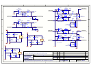
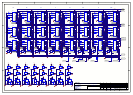
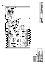
Video PCB Icons + Mechanical
Refer to circuit diagram L922 sheet 1
This sheet contains drawing symbols to enter items on the
run out BOM as well as the chassis fixing points and their
associated EMC decoupling capacitors.
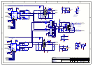
Video Board Top
Refer to circuit diagram L922 sheet 2
This sheet shows the interconnections between the
different sheets within the Schematic Hierarchy. It also
shows the snap off for the Headphone connector.
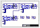
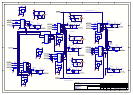
Video Board
Refer to circuit diagram L922 sheet 3
This snap of PCB contains the composite video inputs the
composite multiplexer and the composite outputs and their
mute circuits. The video inputs are 75R terminated then
AC coupled to the inputs of two RHOM BA7625 5 : 2
multiplexers. These multiplexers have a gain of 2 (i.e.
6dB) expect to be AC coupled at the input and DC coupled
at the output, if the input is inadvertently DC coupled it
will shut down as the bias network will not operate. This
could happen if any of the coupling caps are dc short at the
input.
IC 200 is the main signal path multiplexer. Output 1 from
the main multiplexer IC200 goes to the main PCB via the
buffer IC203 and SK209 to the OSD chip. IC 202 is the
VCR videotape loop it is buffered by IC203 then AC
coupled and connected via a 75R series termination
resistor to the RCA phono connector SK201.
IC201 is the Zone 2 multilexer output one from this is fed
via the buffer IC203 and SK209 to the main PCB where it
goes to the Zone 2 OSD chip.
The Buffer chip IC203 is a BA7623 video driver chip from
RHOM, it expects to be DC coupled at the input and AC
coupled at the output. If any DC current is drawn from the
output the chip will shut down as the output bias network
will not work. This could happen if any of the output caps
are DC short.
The monitor 1 and 2 outputs and the Zone 2 output are fed
directly from the main PCB via SK209 to the 75R series
termination resistors, after the termination resistors are the
mute transistors which pull to ground to shut down the
output. This only provides about 20dB of mute however
this is enough to shut down the sync so that a monitor will
not recognise that a signal is present.
The multiplexers are controlled via the serial to parallel
conversion latches IC204 and IC205. These are
programmed by a 16bit data word. The clock for the data
is (Video Serial CLK A) and the DATA is (Video serial
data A), once all sixteen bits have been clocked into the
latch the data is passed to the outputs by clocking the latch
signal video comp latch.
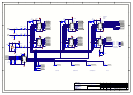
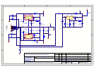
Screen Display
Refer to circuit diagram L922 sheet 4
This sheet contains; the on screen display chip for the
main zone 1, the input multiplexer for the onscreen display
chip to select which type of video source to send to the
OSD, the clock oscillators for PAL and NTSC generation,
the clock multiplexer to select PAL or NTSC for each of
the zones, the RGB output buffers and sync on green
insertion, a sync separator and mono-stable to generate a
black level clamp signal.
IC301 selects the input signal from the composite, S video
or Y/G inputs, this signal is buffered by Q300 divided by
two by the two 75R resistors then AC coupled into the
input of the On Screen Display chip IC302. It is also
possible to route the output of the OSD chip itself via this
multiplexer to the input of the sync separator so that the
black level clamp can still operate when the OSD chip is
generating RGB or YUV signals.
IC302 is the On Screen Display chip it generates the text
patterns which are multiplexed into the video using the fast
blanking signal. Fast blanking is asserted whenever there
is activity on the output of the OSD chip. The chip is
programmed via a serial bus made up of the lines Video
serial data, Video serial clk and Video serial cs. The
Horizontal line lock is performed by a Phase Locked loop
internal to the OSD chip the filter components for which
are R349, C349 and C350.
LESCREEN input sets the screen intensity for the
background and LECHAR sets the Screen intensity for the
Characters. The potential dividers on the pins define the
voltages.
The composite output of the OSD chip is sync tip clamped
by the circuit made up of Q302 Q304 and D300. This
circuit pulls the most negative part of the signal to a fixed
voltage, in this case approximately 0v.
The sync tip clamp works in the following way. A fixed
voltage of approximately 1.2v is generated by D300 and
the 4K7 current limiting resistor R343, this holds the base
of Q304 at 1.2v which in turn holds the base of Q302 at
0.6v. If the voltage on the collector of Q302 goes 0.6 v
below the voltage on the base (i.e. below 0v) the
darlington pairQ302 and Q304 turns on and dumps charge
on the coupling capacitor C348 until the voltage is
increased to 0v. So the most negative part of the signal
always remains at 0v, the most negative part of a
composite video signal is the sync and hence this is pulled
to 0v.
This sync tip clamp circuit is used for all of the composite
signals so they are all clamped to the same level. This